8080 Minicomputer in FPGA
I've always enjoyed learning about antique computers, specifically those from the 8080 to 8088 range. I had a little time on my hands and an FPGA development kit that wasn't doing anything, so I decided to build myself a computer based on the 8080 CPU. I already knew how to build a basic 8080 computer, I had just never gotten around to it because of the time involved, but with an FPGA it wouldn't take the considerable amount of time that would be needed to build it from discrete parts. The finished project has a UART, a GPIO peripheral, and a bootloader in ROM that will download code into RAM over the serial port.
Most of the finished computer consists of code written by other people, I just took the time to integrate it all into something useful and enjoyable.
8080 CPU
I used an 8080 core from opencores.org, written by Scott Moore. I had one major reason for picking it: it was written in Verilog. Scott's project page contains a lot of great information. It was where I found out about S-CS1. Scott's project is a lot more advanced than mine, and contains a complete terminal emulator instead of just a UART and a couple of other peripherals (like an interrupt controller). However, I wanted to have a little more of a hand in the final product so I chose only to use his CPU core.
Memory
The RAM is a simple IP core from Xilinx, generated using CORE Generator. The Virtex-4 has quite a bit of block RAM available, so I was able to generate a memory that filled the entire address space of the 8080 (64k). There's a wrapper around the memory to handle the transition from two uni-directional data busses to the bi-directional data bus used by CPU.
The ROM is 768 bytes and is pre-loaded with a bootloader that I wrote (bootload.asm). There is a memory switcher peripheral that will switch between the ROM and the RAM. On reset or boot-up, the bootloader in ROM is active. Then whatever program that is going to be run is downloaded into RAM and the CPU writes a one to the memory switcher which resets the CPU and disables the ROM.
UART
The transmitter and receiver cores are from fpga4fun.com. I chose them because they were simple, all of the cores available from opencores were either written in VHDL or used the Wishbone bus, which I didn't want to have to deal with decoding. The one issue I have with these cores is that the code is very hard to follow. I had to add some reset logic to the registers to keep the synthesis tool happy, otherwise it had decided it was going to “optimize” them away. If I have some more time in the future I'll replace them completely with my own code. I added a transmit and receive FIFO onto the transmitter and receiver and then wrote some code to provide status signals for the monitor. Supposedly, the status bits emulate a MITS Serial I/O Card (according to Scott on his project page), however, what the status bits indicate doesn't make a whole lot of sense to me, but it's what the software looks for, so I left it as is.
GPIO
I wrote a little GPIO peripheral so I could blink some LEDs and read some switches. It has an 8 bit input port and an 8 bit output port. It's very simple.
Bootloader
Originally, I used CORE files to initalize the RAM. The problem with this approach is two-fold. First, I would have to recompile the entire design after changing the program, so debugging got to be very tedious. Second, this would only work for small programs. If I tried to load any decent sized program, the CORE file got overly large.
Once I started working with large programs, it became obvious that I needed a different solution. After thinking about the problem for a while, I came up with a simple but elegant solution (though I doubt I am the first to think of it, I'm pretty sure this is the same method used in computers of this era to load programs). I wrote a peripheral that would control access to the bootloader ROM and RAM. What happens is that on startup, the ROM is enabled and “placed” at the start of the address space (e.g. address 0000h). A memory read to any address in the ROM address space is read from the ROM. A memory read above the ROM address space is redirected to RAM. A write to any address is sent to RAM. Thus, a bootloader in ROM can run and initialize the RAM without having to exist in the RAM itself (almost, read on…)! The memory peripheral also monitors the IO bus, so a command can be written to its IO register to run the program in RAM. What happens is the memory peripheral will put the CPU into reset and disable all access to the ROM. It then releases the reset and the CPU begins executing the program in RAM like nothing ever happened. On a hard reset, the ROM is once again enabled.
This approach has some limitations. First, because I was too lazy to “unroll” my code I use subroutines, which requires the use of a stack. Obviously, we can't implement a stack in ROM, so the bootloader uses the top 20 bytes of RAM as a stack. To get around this I just made sure that the programs I was loading didn't have any data/instructions located at the very top of the memory. After the program starts running though, it's free to use all of the available memory. Second, I wanted some form of error checking. I figured the easiest solution would be to just have the bootloader read back the memory after a write was performed. One issue presents itself though when we get into the ROM's address space. When the CPU performs a read it will read back the data in the ROM, not the data in the RAM! Initially, this issue presented itself as my Python programmer entering an infinite loop because the data that was read back was never correct. I “fixed” the issue by just having the Python programmer perform no data error checking on addresses in the ROM address space. I know this isn't perfect, but it doesn't bother me too much because there has not been a single data error since I began using the programmer.
Software
Scott included a copy of S-CS1 in his project directory written for his own assembler called IP-PASCAL. I rewrote Scott's copy of the code to work with a different assembler called sbasm, which it seems has faded from the internet. I also changed all the output to upper-case, because I think all classic computers should use upper-case :P. Finally, I added a couple of extra error messages that I used when debugging the code. The final version of the code takes about 3800 bytes of memory. It also uses memory addresses 0x1000 to 0x12FF for RAM. Everything above that is free for the programmer to use. It is called scs1.asm and is included in the project zip below.
The bootloader takes up about half of the 768 byte ROM and has three commands, write, clear, and done. The write command will write a byte of data to an address in RAM, the clear command will clear the RAM, and the done command will reset the CPU and start running the program in RAM. On reset the bootloader will become active again and clear the RAM.
I wrote a programmer in Python that will take the Intel Hex file produced by the assembler and download it to the RAM over the serial port. It is called hextochip.py. It takes one command line argument, the name of the hex file.
I also wrote a little utility in Python that will take the hex file and write a COE file that you can import into CORE Generator. It is called hextocoe.py. It takes two command line arguments, the first is the hex file to read and the second is the coe file for writing. It does not work for large programs, though, because the COE file will get overly large (gigabytes…I'm serious). In this case you have to use the programmer instead.
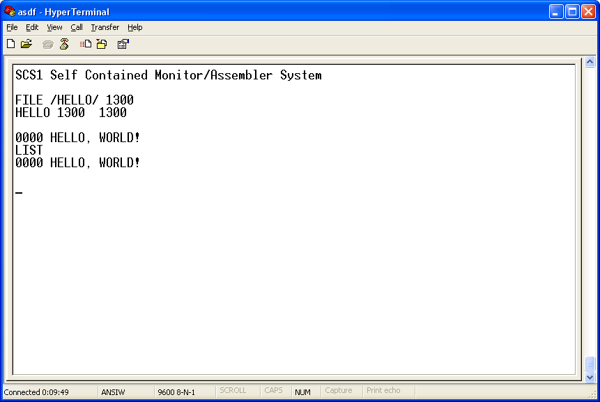
Results
Here is a screenshot of the computer printing a classic message! The final design runs at 10 MHz, which, according to the Wikipedia article, gives it a throughput of 2.5 MIPS!
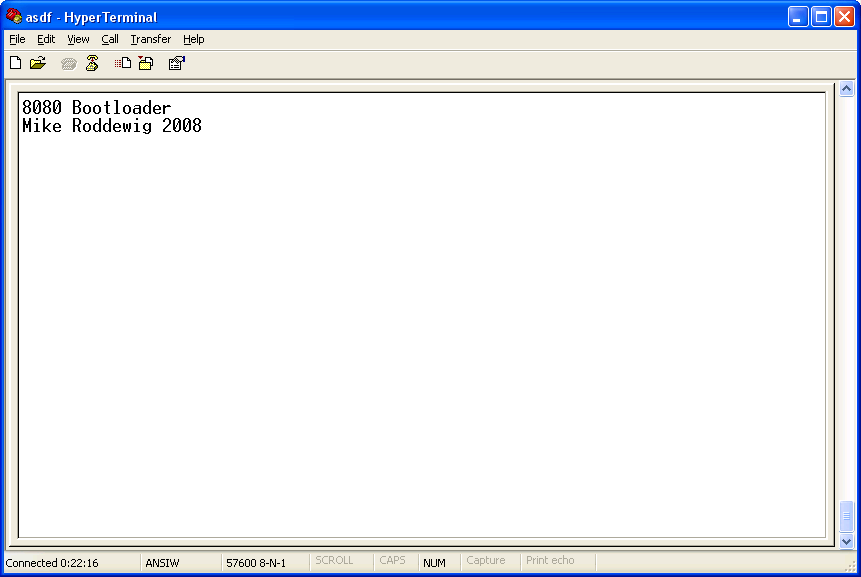
Here is a screenshot of the bootloader.
Files
The Verilog source and Xilinx CORE files as well as the assembly code for S-CS1 and the bootloader are linked below. Also linked are the Python utilities for writing to the RAM and COE files. I also uploaded the manual for S-CS1. The UCF file is written for an ML-402 development board. To use this project in your design you will most likely have to modify the UCF file and change the pin assignments. The top-level Verilog file is called computer.v.
License and Credits
8080 CPU Core
The 8080 CPU was written by Scott Moore. His website is http://www.moorecad.com.
The 8080 CPU implemented here was created as a not for profit student project. I don't know if its use will violate patents, copyrights, trademark rights or other rights. The source files were created entirely by me, but their use, commercial or otherwise, and any legal, consequences that arise, are entirely the responsibility of the user. I specifically deny that this core is usable for life support systems, or any other system that can or will cause, directly or indirectly, any harm to persons or property.
THESE SOURCE FILES ARE PROVIDED “AS IS” AND WITHOUT ANY EXPRESS OR IMPLIED WARRANTIES, INCLUDING, WITHOUT LIMITATION, THE IMPLIED WARRANTIES OF MERCHANTIBILITY AND FITNESS FOR A PARTICULAR PURPOSE.
UART Transmitter and Receiver Cores
The asynchronous transmitter and receiver cores are by Jean P. Nicolle and are Copyright © fpga4fun.com KNJN LLC - 2003, 2004, 2005, 2006. His website is http://www.fpga4fun.com. They are released under the following license.
All the information (including software, designs and files) on this site are provided “as is” and without any warranties expressed or implied, including but not limited to implied warranties of merchantability and fitness for a particular purpose. In no event should the author be liable for any damages whatsoever (including without limitation, damages for loss of business profits, business interruption, loss of business information, or any other pecuniary loss) arising out of the use or inability to use information (including software, designs and files) provided on this site.
Remaining Software
The remaining software is Copyright © 2008, 2011 Mike Roddewig. All rights reserved.
This program is free software: you can redistribute it and/or modify it under the terms of the GNU General Public License v3 as published by the Free Software Foundation.
This program is distributed in the hope that it will be useful, but WITHOUT ANY WARRANTY; without even the implied warranty of MERCHANTABILITY or FITNESS FOR A PARTICULAR PURPOSE. See the GNU General Public License for more details.
You should have received a copy of the GNU General Public License along with this program. If not, see <http://www.gnu.org/licenses/>